Network Publications
If you are a member of the RenewPV Cost network, and you are publishing a paper in the area covered by the network, please could you acknowledge the action with the following text :
This article/video/podcast/webinar/animation/presentation is based upon the work from COST Action RenewPV CA21148, supported by COST (European Cooperation in Science and Technology).

Lynch, T., López, C., Cazorla, C., & McKenna, K. P. (2026). Structural and Electronic Reconstruction of Extended Defects in Pnictogen Chalcohalides. The Journal of Physical Chemistry Letters.
https://doi.org/10.1021/acs.jpclett.5c03107
Abstract
With growing global demand for renewable energy, thin-film photovoltaic technologies are emerging as a promising route to low-cost, scalable solar power. However, for many candidate materials extended defects in polycrystalline thin films are associated with deep gap states that limit carrier lifetimes and reduce device efficiency. Pnictogen chalcohalide semiconductors with the general formula MChX (M = pnictogen, Ch = chalcogen, X = halogen) have been proposed as defect-tolerant alternatives. Using density functional theory, we predict the structure and electronic properties of surface defects for eight pnictogen chalcohalide compounds and analyze their behavior upon surface reconstruction. Our results reveal that, despite the cleavage of covalent bonds, these materials undergo reconstructions that eliminate detrimental gap states. The facile formation of new interchain bonds at the surface preserves the electronic performance of the materials and suggests intrinsic resilience to extended defects. These findings position pnictogen chalcohalides as promising candidates for defect-tolerant, stable, thin-film photovoltaic absorbers.

Abasi Abudulimu, Xiaoming Wang, Tyler Brau, Jaroslav Kuliček, Scott L. Wenner, Adam B. Phillips, Ebin Bastola, Manoj K. Jamarkattel, Vijay C. Karade, Kiran Lamichhane, Aparajita Dixit, Bohuslav Rezek, Yanfa Yan, Michael J. Heben, Randy J. Ellingson (2026). Radiative Defects in Chloride-Activated CdSe Thin Films. ACS Energy Letters.
Abstract
Defect recombination limits wide-gap Se-based chalcogenide devices, yet how chloride activation reshapes radiative pathways remains unclear. Here we show that a 40 min CdCl2 anneal converts evaporated CdSe from porous nanograins into dense micrometer-scale polycrystals and sharpens the optical band edge, reducing the Urbach energy from 85 to 17 meV at 300 K. Combining temperature- and fluence-dependent photoluminescence (PL), time-resolved PL, hyperspectral mapping, and hybrid-DFT, we resolve three emissive channels and identify their mechanisms. The near-edge band is excitonic at low temperature and evolves into free-carrier emission at elevated temperature. A sub-gap band at Eg −0.45 eV requires above-gap carriers and thermally quenches with a 0.16 eV activation energy. A broad ∼1.05 eV infrared band is excited by above- and below-gap photons and retains microsecond lifetimes at room temperature; patial mapping links it to edge-rich microstructure. Calculations suggest selenium-vacancy and cadmium-vacancy–chlorine complexes, pointing to routes to suppress defect-related losses in wide-gap chalcogenide devices.

Medina, S., Nezzari, A., Guezzoul, M. et al. Molecular Ink Spray-Coated Cu2CoSnS4 Thin Films as Non-Toxic, Sulfurization-Free absorbers for Solar Cells. Braz J Phys 56, 2 (2026). https://doi.org/10.1007/s13538-025-01918-3. https://doi.org/10.1002/pip.3899
Abstract
We fabricated Cu₂CoSnS₄ (CCTS) thin films using spray-coating with a dimethylformamide-based molecular ink, deposited at 100 °C and 140 °C, and annealed at 360 °C in air. X-ray diffraction and Raman spectroscopy confirmed the stannite structure, with improved crystallinity and fewer impurities at 140 °C. The films show promise as non-toxic, sulfurization-free absorber layers for solar cells, with tunable optical and electrical properties. X-ray photoelectron spectroscopy (XPS) revealed temperature-dependent shifts in chemical composition and oxidation states. These shifts indicate altered stoichiometry at higher temperatures. Morphological analyses through SEM and AFM showed increased grain size, improved uniformity, and enhanced surface roughness with higher deposition temperatures. Energy-dispersive X-ray (EDX) mapping confirmed uniform elemental distribution, with deviations from ideal stoichiometry observed at 140 °C. Optical studies indicated a reduction in the band gap from 2.06 eV at 100 °C to 1.64 eV at 140 °C. The electrical measurements via Hall Effect show that all films exhibit a transition from p-type conductivity at 100 °C (carrier concentration of 1.057 × 101⁰ cm⁻3, mobility of 32.85 cm2/V.s, and resistivity of 8.994 × 10² Ω.cm) to n-type conductivity at 140 °C (carrier concentration of -2.486 × 10⁶ cm⁻3, mobility of 80.26 cm2/V.s, and resistivity of 3.098 × 10⁴ Ω.cm).These findings highlight the promise of CCTS films as environmentally friendly, sulfurization-free absorber layers for thin-film solar cells and optoelectronic applications, emphasizing the crucial role of deposition optimization in achieving enhanced material properties.

El Kanouny, A., Elotmani, R., El Manouni, A., El Khouja, O., Assahsahi, I., Almaggoussi, A., & Galca, A. C. (2025). Electrodeposition of SnSe nanosheets: Effect of deposition potential on structural, morphological, and optical properties. Applied Physics A, 131(12), 979. https://doi.org/10.1016/j.ceramint.2025.08.041
Abstract

El Khouja, O., Popescu, B., Assahsahi, I., Negrila, C. C., Leonat, L. N., Nouneh, K., … & Galca, A. C. (2025). Improved Sulfurization Process for Enhancing the Microstructure and Transport Properties of Spray Pyrolysis-Deposited Cu2ZnSnS4 Films. Ceramics International. https://doi.org/10.1016/j.ceramint.2025.08.041
Abstract

Tamin, M., El Khouja, O., Guemmaz, M., Tamin, C., Bocirnea, A. E., Asshsahi, I., … & Galca, A. C. (2025). Towards a wide bandgap absorber: structural, morphological, and optical investigation of Ag-alloyed Cu 2 ZnSnS 4 thin films. Sustainable Energy & Fuels. https://doi.org/10.1039/D5SE01303H
Abstract

Miliaieva, D., Nadazdy, V., Koltsov, M., López, C., Saeeyekta, H., Kuliček, J., … & Spalatu, N. (2025). Electronic structure and defect states in bismuth and antimony sulphides identified by energy-resolved electrochemical impedance spectroscopy. Journal of Physics: Energy, 7(3), 035012. https://doi.org/10.1088/2515-7655/add59f
Abstract

Outman El Khouja, Yuancai Gong, Alex Jimenez-Arguijo, Maykel Jimenez Guerra, Axel Gon Medaille, Romain Scaffidi, Arindam Basak, Cristian Radu, Denis Flandre, Bart Vermang, Sergio Giraldo, Marcel Placidi, Zacharie Jehl Li-Kao, Aurelian Catalin Galca, Edgardo Saucedo. (2025). Exploring the Synthesis of Cu2 (Zn, Cd) SnS4 at High Temperatures as a Route for High‐Efficiency Solar Cells. Progress in Photovoltaics: Research and Applications, 33(5), 628-643. https://doi.org/10.1002/pip.3899
Abstract
The present research explores for the first time the intricate relationship between sulfurization temperature at unusual high temperatures (up to 700°C) and the structural/optoelectronic properties of Cu2(Zn,Cd)SnS4 (CZCTS) thin films, synthesized via a two-step sequential process involving the precursor film deposition using aprotic molecular ink followed by thermal treatment in sulfur atmosphere. X-ray diffraction patterns confirms the tetragonal structure. Scanning Electron Micrographs revealed significant grain growth, with grain sizes increasing from ~0.3 μm at 620°C to ~1.5 μm at 680°C, effectively reducing grain boundary recombination. Energy dispersive X-ray spectroscopy demonstrated a Cu-poor and Zn-rich composition, with a consistent Cd incorporation of ~3.7 at%. Raman spectroscopy showcases the homogeneity and purity of the CZCTS crystalline structure. Precise control of the sulfurization temperature plays a crucial role in determining the photovoltaic characteristics of CZCTS-based solar cells. By increasing the grain size and preventing the thermal decomposition of the CZTS phase, the photovoltaic performance peaked at a sulfurization temperature of 680°C, achieving a power conversion efficiency (PCE) of 10.4%, with an open-circuit voltage of 0.701 V, a short-circuit current density of 24.3 mA/cm2 and a fill factor of 60.8%. External quantum efficiency reached a maximum of 83.3% at 580 nm. The bandgap of the CZCTS absorber was determined to be 1.48 eV, optimal for photovoltaic applications. However, further increasing the sulfurization temperature to 700°C resulted in a lower PCE of 8.5%, attributed to interface degradation and secondary phase formation. Temperature-dependent current–voltage measurements revealed a reduction in recombination losses, with an activation energy of 1.24 eV at the CZCTS/CdS interface, indicating effective defect passivation by Cd incorporation. The optimized films, sulfurized at 680°C, displayed an absorber thickness of ~1.2 μm after sulfurization, providing efficient light absorption and charge transport. The findings not only emphasize the critical role of sulfurization temperature in engineering CZCTS film and subsequently their functionality but also provide valuable insights for fine tuning their performance in the field of photovoltaic applications.

Baghirov, Mahammad Baghir and Muradov, Mustafa and Eyvazova, Goncha and Azizian-Kalandaragh, Yashar and Mammadyarova, Sevinj and Kim, Jiseok and Gasımov, Eldar and Rzayev, Fuad. Effect of sulphidation process on the structure{,} morphology and optical properties of GO/AgNWs composites. RSC Adv., 2024, 14 (4), pp. 2320-2326. The Royal Society of Chemistry. http://dx.doi.org/10.1039/D3RA08044G
Abstract
In this study, composite materials composed of graphene oxide (GO) synthesized by a modified Hummers’ method and silver nanowires (AgNWs) synthesized by a modified polyol method were prepared. The prepared composites were subjected to sulfidation under the influence of H2S gas. Structural changes in the samples were evaluated using X-ray diffraction (XRD). The binding nature of the composite was characterized using FT-IR spectroscopy. Optical properties and band gap values were investigated using ultraviolet-visible (UV-Vis) spectroscopy. The morphology of the composites was analyzed by transmission electron microscopy (TEM). A simple method using H2S gas was applied for the sulphidation process of the samples. The sulfidation process was successful under the influence of H2S gas, resulting in an increased distance between the GO layers and a decrease in the band gap value for the composite post-sulfidation. In addition, AgNWs were observed to decompose into Ag2S nanoparticles under the influence of H2S gas. It was determined that the value of the band gap of the sample changes because of sulphidation.
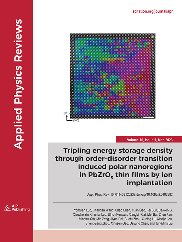
J. Quirk, M. Rothmann, W. Li, D. Abou-Ras, K. P. McKenna; Grain boundaries in polycrystalline materials for energy applications: First principles modeling and electron microscopy. Appl. Phys. Rev. 1 March 2024; 11 (1): 011308. https://doi.org/10.1063/5.0175150
Abstract
Polycrystalline materials are ubiquitous in technology, and grain boundaries have long been known to affect materials properties and performance. First principles materials modeling and electron microscopy methods are powerful and highly complementary for investigating the atomic scale structure and properties of grain boundaries. In this review, we provide an introduction to key concepts and approaches for investigating grain boundaries using these methods. We also provide a number of case studies providing examples of their application to understand the impact of grain boundaries for a range of energy materials. Most of the materials presented are of interest for photovoltaic and photoelectrochemical applications and so we include a more in depth discussion of how modeling and electron microscopy can be employed to understand the impact of grain boundaries on the behavior of photoexcited electrons and holes (including carrier transport and recombination). However, we also include discussion of materials relevant to rechargeable batteries as another important class of materials for energy applications. We conclude the review with a discussion of outstanding challenges in the field and the exciting prospects for progress in the coming years.
Abstract
Antimony trisulfide (Sb2S3) is a promising photovoltaic absorber, which has so far been fabricated mainly by chemical deposition methods. Despite its aptness for congruent sublimation, less research efforts have been made on low-temperature Sb2S3 processing by physical methods. In this regard, recent studies show large variation in the processing temperature of Sb2S3 films, which overall brings into question the need for higher substrate temperatures (>350 °C). Furthermore, in-depth analysis of defect structure of Sb2S3 employing temperature-dependent admittance spectroscopy (TAS) and photoluminescence (PL) remains largely unexplored. In this work, we systematically study the effect of close-spaced sublimation (CSS) substrate temperature on Sb2S3 absorber growth, employing a wide temperature range of 240–400 °C. Temperatures above 320 °C caused cracking phenomena in the Sb2S3 absorber film, proving the unviability of higher processing temperatures. CSS processing temperature of 300 °C was found optimal, producing crack-free Sb2S3 films with increased presence of (hk1) planes, and achieving the best CdS/Sb2S3 device with photoconversion efficiency of 3.8%. TAS study revealed two deep defects with activation energies of 0.32 eV and 0.37 eV. Low-temperature PL measurement revealed a band-to-band emission at 1.72 eV and a broad band peaked at 1.40 eV, which was assigned to a donor-acceptor pair recombination. Temperature-dependent I-V analysis showed that recombination at CdS–Sb2S3 interface remains a large limitation for the device efficiency.
Ali Sadek Kadari, Abdelkader Nebatti Ech-Chergui, Prashant R. Ghediya, Atika Guendouz, M’hamed Guezzoul, Outman El Khouja, Amelia Elena Bocirnea, Kouider Driss-Khodja, Bouhalouane Amrani, Aurelian Catalin Galca, Materialia, 2024, 36, 102178, https://doi.org/10.1016/j.mtla.2024.102178
Abstract
Quaternary multicomponent Cu2BaSnS4 (CBTS) has emerged as a potential absorber material due to its abundant and nontoxic constituents, high absorption coefficient (10−4 cm−1) and suitable bandgap (1.5–2.0 eV) for the solar photovoltaic application. In this study, polycrystalline CBTS thin layers have been deposited by a typical spray pyrolysis technique on glass substrates using different substrate temperatures (Ts = 200, 250, 300 and 350 °C) followed by annealing in a sulfur-rich atmosphere at 550 °C under an argon flow. The (micro-)structural, compositional, and optical properties of both types of films have been studied. Analysis of x-ray diffractogram (XRD) patterns for all acquired films showed the presence of polycrystalline CBTS alongside various secondary phases, including Cu2SnS3 being predominant. Nonetheless, the XRD of the films deposited at 250 °C and annealed at 550 °C showed only the CBTS phase. Raman spectroscopy confirm the formation of the trigonal phase of CBTS. The presence of Cu, Ba, Sn and S in CBTS thin films was confirmed by X-ray photoelectron spectroscopy and Energy-dispersive X-ray spectroscopy. Scanning electron micrographs show a smooth and dense structure with enhanced crystallinity and improved uniformity. Overall, the physical properties of CBTS thin films were found to be spray deposition temperature dependent. An appropriate optical band gap of 1.6 to 1.8 eV and a compact structure indicate their prospective for solar cell applications.
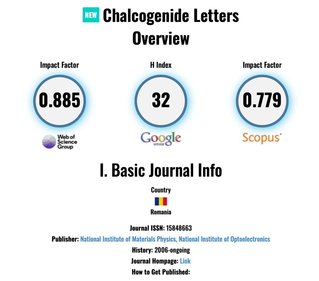
L.R. Gahramanli, S. Bellucci , M. B. Muradov , M. La Pietra , G. M. Eyvazov , C. V. Gomez , J. Bachmann; Chalcogenide Letters, Vol. 21, No.7, July 2024, p.513-527.
Abstract
A new type of Ag2S-CdS/Ag/GNP nanocomposite material was successfully synthesized in the presented work. The structural and physical properties of compounds were studied separately and together. Ag2S-CdS/Ag/GNP nanocomposite materials were studied by Xray diffraction (XRD), Ultraviolet-Visible (UV-Vis), Fourier Transform Infrared (FTIR), Raman spectroscopy and Scanning Electron Microscopy (SEM). Based on the results, Ag nanowires (NWs) were successfully synthesized, and then it was determined that during the hybridization process, two phases of acanthite Ag2S and the cubic crystal system of Ag2O were formed. Then, Ag2S-CdS NWs were formed from mixed monoclinic Ag2S and hexagonal CdS. In the absorption spectrum of Ag NWs, the main absorbance peaks were observed at 357.3 nm and 380.2 nm. The energy gap (Eg) values of the Ag sample are 3.8 eV. The band gap value of Ag2S (2.5, 3.8, 4.6 eV) and Ag2S-CdS (2.5, 3.8, 4.8 eV) have a triple value due to the formation of a hybrid structure. The Raman spectrum of Ag2S-CdS belongs to longitudinal-optical (LO) phonon modes of zinc-blende phase CdS and for the 1, 2, and 3 times spin-coated samples on the surface of GNP/PVA have observed all characteristic Raman peaks, which belong to NWs at 485.13 cm-1, and 960.22 cm-1.

Elyazid El Mahboub, Outman El Khouja, Amelia Elena Bocirnea, Sana Zakaria, Aurelian Catalin Galca, Mohammed Mansori, Ahmed El Hichou
Applied Surface Science 2024, 672, 160848
https://doi.org/10.1016/j.apsusc.2024.160848
Abstract
In this study, the Cu2Zn1-xCoxSnS4 (CZn1-xCoxTS) films with partial cation substitution of cobalt are synthetized by sol gel spin coating, followed by sulfurization treatment. The incorporation of cobalt cation in the CZTS crystalline lattice as well as the phase transition from kesterite to stannite were confirmed by the X-ray diffraction (XRD) and Raman spectroscopy data. The XRD pattern shows peak-shifting toward higher 2θ by increasing the Co concentration, indicating a decrease in lattice parameters. The red shift of Raman peaks by increasing x from 0 to 0.6, confirms the phase transition. The CZn1-xCoxTS morphology was observed by scanning electron microscopy, showing large grain size as x increases and a good distribution of elements for all films. X-ray photoelectron spectroscopy was employed to study the valence of cations/anions and to probe the chemical bonds. The optical band gap showed a parabolic behavior versus the molar ratio Co/(Co + Zn), this deviation from Vegard’s law being induced by the difference in electronegativity between cobalt and zinc. The pure CZTS has a band gap of 1.47 eV, while for CZn0.6Co0.4TS the gap is 1.17 eV, which indicates that the incorporation of cobalt cation produces a red-shift of the band to band transition energy.

Nuriyeva, S., Karimova, A., Shirinova, H., Jafarova, S., Abbas, G., Zamchiy, A., & Aguas, H. (2024).
Micromachines, 15(11), 1318.
Abstract
The production of cost-effective novel materials for PV solar cells with long-term stability, high energy conversion efficiency, enhanced photon absorption, and easy electron transport has stimulated great interest in the research community over the last decades. In the presented work, Cu/Cu2S-MWCNTs nanocomposites were produced and analyzed in the framework of potential applications for PV solar cells. Firstly, the surface of the produced one-dimensional Cu was covered by Cu2S nanoflake. XRD data prove the formation of both Cu and Cu2S structures. The length and diameter of the one-dimensional Cu wire were 5–15 µm and 80–200 nm, respectively. The thickness of the Cu2S nanoflake layer on the surface of the Cu was up to 100 nm. In addition, the Cu/Cu2S system was enriched with MWCNTs. MWCNs with a diameter of 50 nm interact by forming a conductive network around the Cu/Cu2S system and facilitate quick electron transport. Raman spectra also prove good interfacial coupling between the Cu/Cu2S system and MWCNTs, which is crucial for charge separation and electron transfer in PV solar cells. Furthermore, UV studies show that Cu/Cu2S-MWCNTs nanocomposites have a wide absorption band. Thus, MWCNTs, Cu, and Cu2S exhibit an intense absorption spectrum at 260 nm, 590 nm, and 972 nm, respectively. With a broad absorption band spanning the visible–infrared spectrum, the Cu/Cu2S-MWCNTs combination can significantly boost PV solar cells’ power conversion efficiency. Furthermore, UV research demonstrates that the plasmonic character of the material is altered fundamentally when CuS covers the Cu surface. Additionally, MWCN-Cu/Cu2S nanocomposite exhibits hybrid plasmonic phenomena. The bandgap of Cu/Cu2S NWs was found to be approximately 1.3 eV. Regarding electron transfer and electromagnetic radiation absorption, the collective oscillations in plasmonic metal-p-type semiconductor–conductor MWCNT contacts can thus greatly increase energy conversion efficiency. The Cu/Cu2S-MWCNTs nanocomposite is therefore a promising new material for PV solar cell application.
